Oscilloscope
Project started on 2005-12-21
Project completed on 2006-01-14
First of all, many thanks to Professor Iravani for teaching us the analysis of linear systems, Professor Wang for her patient tour of digital logic and Verilog. To all the lab TA's for tips on debugging circuits and practical insights. To Mr. Rundle for introducing me to C/C++ and of course, Mr. van Bemmel for showing me the door.
Motivation
Not everyday does one feel the urge to build an oscilloscope. There were many motivating factors. My experience with oscilloscopes began with an old analog machine in the "bowling alley" of my high school, Marc Garneau CI. I just remember how tedious it was to get the thing to show a trace. And then to trigger properly. Upon comparing the results with known values, I realised that the oscilloscope was off vertically and horizontally (i.e. not calibrated). And the probes were so oxidized. One couldn't quite understand why it wouldn't work. So many pains. But there was excitement when the darn thing finally worked and you could see the Lissajous curves or the capacitor charging and discharging. And then, there was these awesome shiny new digital oscilloscopes in the electrical engineering and physics labs at University of Toronto. They even had an auto set function. I mean, how cool is that? You didn't have to fiddle with the knobs anymore, it just worked. I immediately knew what I wanted for Christmas or my birthday. Looking in the Allied Electronics and Newark in One catalogues, I found out that that was out of question.
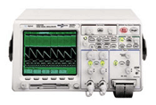
The Agilent 54622D 100MHz mixed signal scope. Such a beauty, no? Starting from $5995USD.
So my natural instinct is to build one if I can't afford one. And thats what I spent my Winter holidays doing.
Requirement Specs
These were the preliminary requirements that I set out to fulfill:
- 1 channel (or 2 channels with common ground)
- It seemed hard to have 2 channels working in electrical isolation
- Digital
- I don't have a CRT or know how to control one
- Communicate to a computer / Palm Pilot via RS232
- For easy debugging and display, a computer is fast and easy to program
- Also allows for future interface with Palm Pilots and easy porting to other systems
- Accuracy of 1mV
- +5V to -5V input range
- 8ksps
- Restricted by ADC0804
- Ampilifcation circuit have relatively high cut off frequency (40KHz suggested)
- Relatively high compared to the 4kHz (nyquist frequency of 8ksps)
Explanation
For those of you who are new to this stuff, here's what the requirement specs mean.
The number of channels which an oscilloscope has is the number of signals which it can be viewed at the same time.
I hope you know what digital and analog means. For the purpose of this project, digital signals can be communicated with computers while analog signals can't.
RS232 is the name given to your serial port. At the back of your computer, there's many ports where you can plug things into. The RS232 port has 9 pins and looks like:
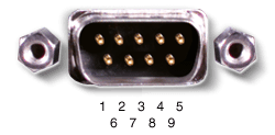
RS232 serial port
At the heart of most digital oscilloscopes is a device (usually a chip of some sort) which converts analog voltage levels to digital signals. This chip is called an analog to digital converter (ADC). If this happens very quickly and the computer keeps track of voltage over time, a plot can be drawn, hence the principal of a digtal oscilloscope. How quickly the chip is able to make these conversions is called the sampling frequency. It is given in units of ksps (kilo-samples per second) or Msps (mega-samples per second). And if you know the sampling frequency to be f, the highest frequency sine wave it can detect is f/2. This is known as the nyquist frequency. Any higher than that and all you'll get erroneous results and an effect known as aliasing (click here for details). For my case, I chose ADC0804 because they are readily availible at Supremetroncis. This chip is guarenteed to work at 8ksps. And hence, the nyquist frequency is 4kHz. That means, the fastest sine wave I can see with chip is 4kHz before bad things start happening.
Most oscilloscopes have some analog circuit which will amplify and shift the trace before it is sampled by the ADC. By shifting the signal before amplifying it gives better accuracy in many cases (avoid saturation with amplifiers). As with all analog circuits, they will work only within a range of frequencies. After a specific frequency, the cut off frequency, the output voltage level is less than 70.7% of the original voltage level and is considered unsuitable for measurement. It would be preferrable for this frequency to be much higher than the nyquist frequency of the ADC.
So, now that we know what we're looking for, here's the design.
Design
While I had some knowledge of electronics hardware, I still do not understand all components fully. It is very different to sketch an opamp circuit on paper than it is to choose the correct components and lay it out to minimize noise. So, there's bound to be oversights where a resistor value was too low or the components were not well chosen, etc. Hence the difference between physics where it supposed to work and engineering were good approximations and correct components are key. I'm still learning so please contact me with comments and suggestions.
The design of this oscilloscope was simple. It is summarized with the following diagram.
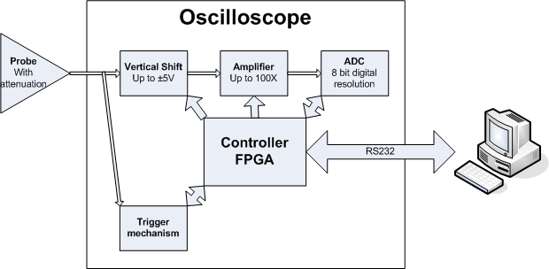
Flow diagram for the digital oscilloscope
Vertical Shift and Amplifier
The purpose of these modules is to condition the signal appropriately for the ADC to read. The ADC can convert voltages within the range of 0 to 5V. By setting the vertical offset and amplification, one can "zoom" into a portion of the signal one is interested in. A suitable equation relating the input voltage (Vin), vertical offset (Vs), amplification (A) and the output voltage to the ADC (Vadc) can be:
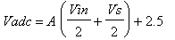
which would allow for the maximum of 10V input range (A=1, Vs=0, Vin=-5V to +5V). Also, this scope must have accuracy of 1mV. The typical screen size on a Palm Pilot is 160X160 pixels. Hence a 100X100 pixel window with 10X10 grid would be suitable for showing the trace which leaves enough space to display system information. This means, the smallest range this oscilloscope should be able to capture is within a 0.1V (=100px X 1mV/px) range. It would also be nice to have variable gain inbetween these two ranges as well. The following table lists the magnifications posible.
| Volts per Div (mV) |
Measurable Window (V) |
Amplification Needed (X) |
Feedback Resistor (see circuit, Rf) (kΩ) |
Multiplexer Index |
|---|---|---|---|---|
| 0.01 | 0.1 | 100 | 1000 | 0x6 |
| 0.02 | 0.2 | 50 | 500 | 0x5 |
| 0.05 | 0.5 | 20 | 200 | 0x4 |
| 0.1 | 1 | 10 | 100 | 0x3 |
| 0.2 | 2 | 5 | 50 | 0x2 |
| 0.5 | 5 | 2 | 20 | 0x1 |
| 1 | 10 | 1 | 10 | 0x0 |
With the design equation in mind, an opamp circuit was created to perform the desired amplification. This was done by cascading a series of buffers, differential amplifiers and summing amplifiers. The result was:
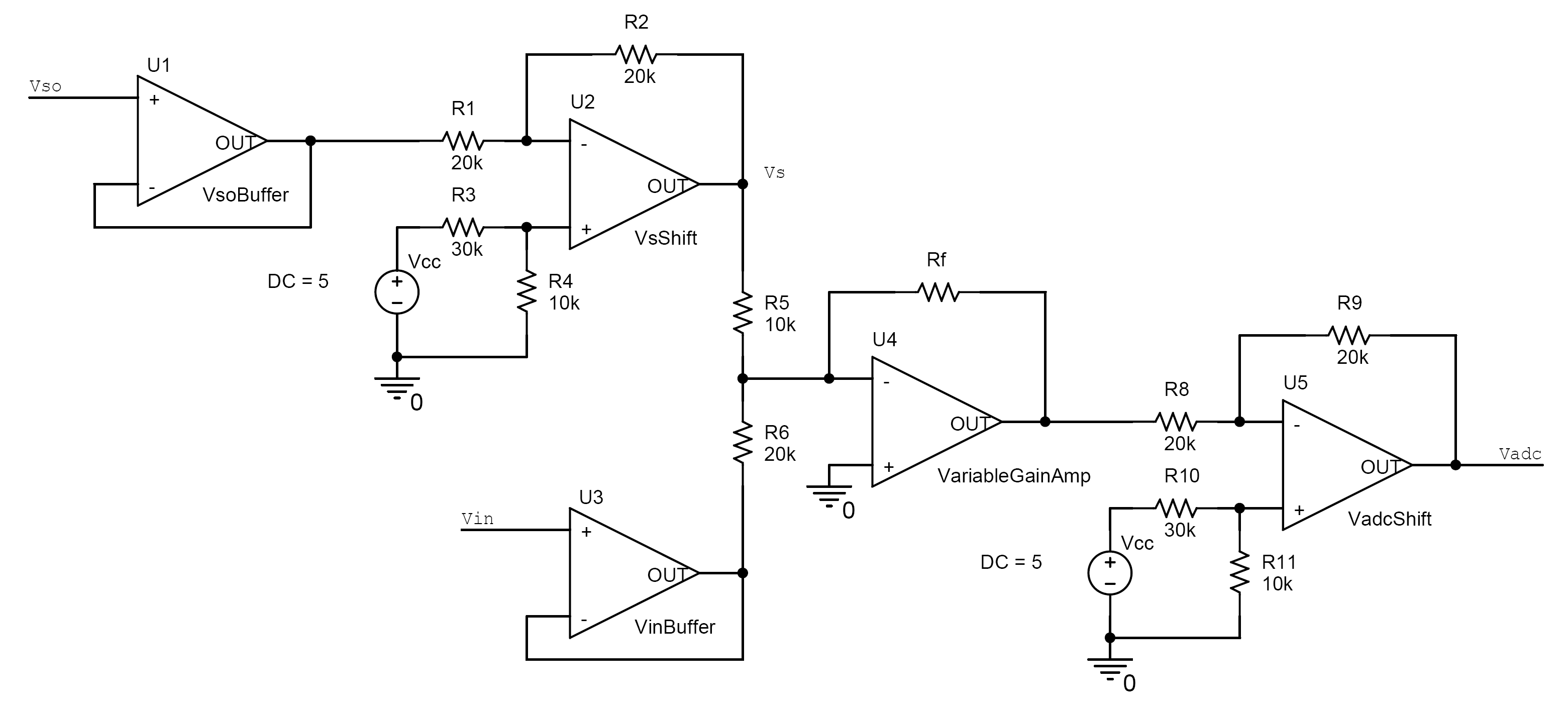
Click on image for higher resolution schematic
Originally, 10k resistors were chosen for most of the circuit since resistors with values in multiples of 10k were most common. This would be useful for the variable gain circuit. However, Supremetronics ran out of them and I was out of luck. So 20k were used instead. I salvaged a few 10k resistors from old projects and used those. Due to the sensitive nature of this project, all resistors had 1% tolerance.
The opamp chosen was the LF347. It has high bandwidth of 4MHz, input impedance of 10e12Ω. Each package contained 4 opamps which saved space and came at an economic price. I'm sure that was not the best reason to pick this opamp, but it still worked.
The variable gain amplifier must be able to accomodate 7 distinct amplification levels. This meant, Rf could be 7 independant values. This was accomplished by using a 4067 which was a 16 to 1 analog multiplexer IC which was not shown on the schematic. Based on the input to the IC, Rf could be configured to choose any of the 16 channels. Since 7 resistors were used, only 7 channels were used and 3 of the 4 lines were needed to address each channel.
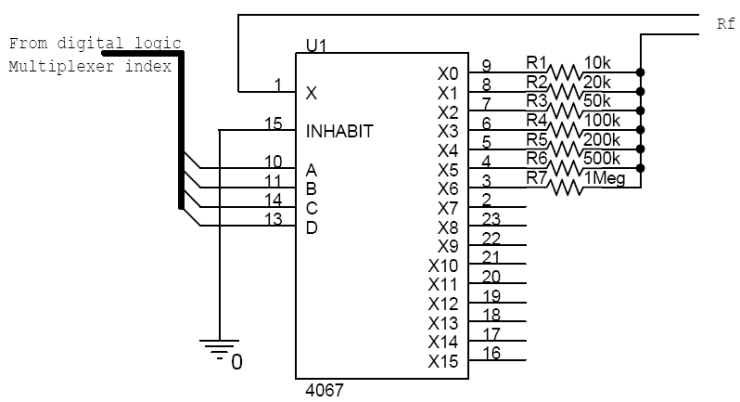
Wiring diagram to create Rf from a 4067
Looking at the circuit, you may notice that there is a physical input signal called Vso which was not mentioned in the design equaiton. This voltage is generated by an R-2R resistor network driven by a CMOS buffer. Hence its voltage range is between 0 and 5V. The logical vertical offset (Vs) can be calculated using Vs=5-2Vso. However, doing a full circuit analysis will reveal that the the design equation still holds.
R-2R networks are constructed using resistors. They are a type of DAC (digital to analog converter). They can convert a digital signal into an analog voltage level. Say an n bit unsigned integer was to represent a voltage level, Vout, between 0 and Vcc. An R-2R resistor network could be constructed to do this as the following:
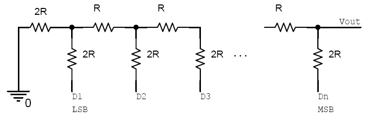
General R-2R network
Every resistor labeled R must all have the same arbitrary resistance. Every resistor labeled 2R must have twice that resistance. For a CMOS circuit, a logical high is Vcc, usually 5V and a logical low is 0V. Doing a circuit analysis, one will find that Vout can be described as:
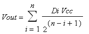
where Di is 1 or 0 and Vcc is the supply voltage to the CMOS driver.
Most CMOS buffers are capable of outputing a maximum of 20mA. So, resistor value for R must be chosen in the kΩ's. This circuit fails miserably if one were to use TTL gates as the voltage levels for high and low have too wide a range. I once read a 2.2V for a logical low out of a 74LS04 (NOT gate). So, you must use CMOS outputs to drive this circuit. The most precise resistors have tolerance of 1%, so excessive number of bits may not guarentee such precision, but the voltage levels will always be ascending if the input values are consecutively ascending.
The requirements demand 1mV accuracy over a 10V range. Doing the calculations, it was found that the size of the output integer needs to be 14 bits. This seems some what inconvenient, so it was rounded up to 16 bits for ease of computation on the computer side at the expense of 4 more resistors.
Power Supply
Like all electrical circuits, this one needs electricity to work. The opamps need a positive and negative voltage source to work. The precision of these two voltages must be very precise and symetric otherwise, the virtual ground would be off (different from the real ground) and this would introduce significant amount of error in the final signal.
For this project, I used a modified ATX power supply. The one in my computer was getting noisy so I replaced it with a new one although the old one was still functional. ATX power supplies can output +12V, +5V, +3.3V, -5V, -12V relative to common ground. So, instead of spending a lot of money on a lab power supply, I used an ATX power supply instead.
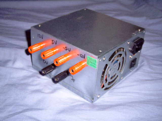
Modified ATX power supply
But measuring the +12V and -12V, I found out that the power supply was not so precise. To make matters more complicated, the voltage level changed when one loaded the power supply which was due to do with the switching nature of computer power supplies. To make a more precise power supply, the following circuit was made (design taken from a voltage regulator datasheet):
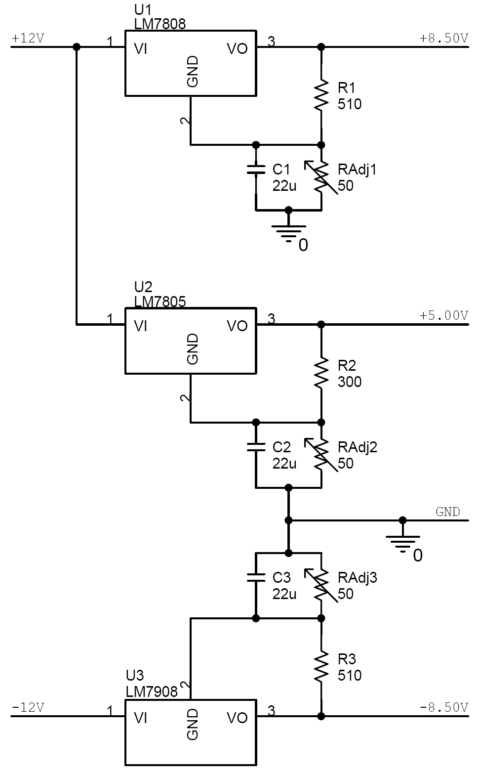
Click on image for higher resolution schematic
This power supply was loaded and the adjustable resistors were trimmed until the desired voltages were obtained.
Digital Logic
Most of the digital circuitry was implemented on an FPGA. If done with simple logic gates and baud generators and all, this project would have been a lot harder and taken a whole lot longer. Plus it gave me an opportunity to practice my Verilog.
Being a student, I did not have much money to spend on an FPGA development board. And I needed something with a serial interface. Looking around the web, I came across Jean's website fpga4fun which became an indespensable resource to this project. I bought the Pluto development board which was surprisingly powerful for its size. Compared the the Altera UP2 board retailing for $180CAD, I got a Pluto board for $80CAD after all S/H fees and taxes. Although it did not have as many features, it did have the most bang for the buck. The Pluto board came with an Acex1k FPGA. It has an on board 27MHz clock an LED and most importantly a serial interface.
All Verilog code was written, compiled and simulated in Quartus II. Sources should be view with hard tabs 4 spaces wide.
Asynchronous Serial Transceiver
These libraries were used to provide connectivity with a computer over the RS232 interface.
Many thanks to Jean for providing his libraries to us. The concept behind asynchronous communications does not seem hard but the Verilog code sure looks confusing. For details, visit http://www.fpga4fun.com/SerialInterface.html. To interface the Pluto FPGA board through the serial port, I used the source code provided in the Appendix of the Getting started with the Pluto boards manual. The source code for that is listed in Pluto.cpp in the source zip file. To port this to Linux, try using something like http://www.yudit.org/uc/pluto.cpp.
SerialRxManager
The purpose of this module is to recieve and process simple commands received over the RS232 interface.
This module instantiates an instance of the serial receiver module. Inside the this manager are 16 four bit registers (total of 64 bits) which control the behaviour of the oscilloscope. These registers can be altered by sending bytes to the Pluto board. Each byte sent is divided into 2 nibbles. The upper nibble contains the address of the register to be modified and the lower nibble contains the new value to be stored in that register. Hence to change the vertical offset, one would have to send 4 bytes (4X4=16 bits).
OutputManager
The purpose of this module is to increase the number of outputs from the Pluto board.
The Pluto board has only 39 pins available for IO. This may seem like a lot, but in reality it isn't. The vertical shift and trigger voltages each need 16 pins. The variable gain requires 3 outputs and the ADC requires 10 pins. This comes out to 45 pins which we don't have. So, in order to decrease the number of pins needed on the FPGA, I multiplexed output to 5 seperate latches repetitively. Although I used latches (due to availability and cost again), in theory, positive or negative edge flip flops should work as well. So, I ended up outputing the vertical shift, trigger level and amplification levels this way. These outputs were not time critical so having a longer propagation delay is not a big deal. This meant, I could drive 40 outputs with 13 pins and freed up 27 pins.
Registers U1 (lower byte) and U2 (higher byte) comprised of 16 bits which generated the vertical offset. Registers U3 (lower byte) and U4 (higher byte) comprised of 16 bits which generated the trigger voltage. U5's output selected Rf for the variable gain amplifier.
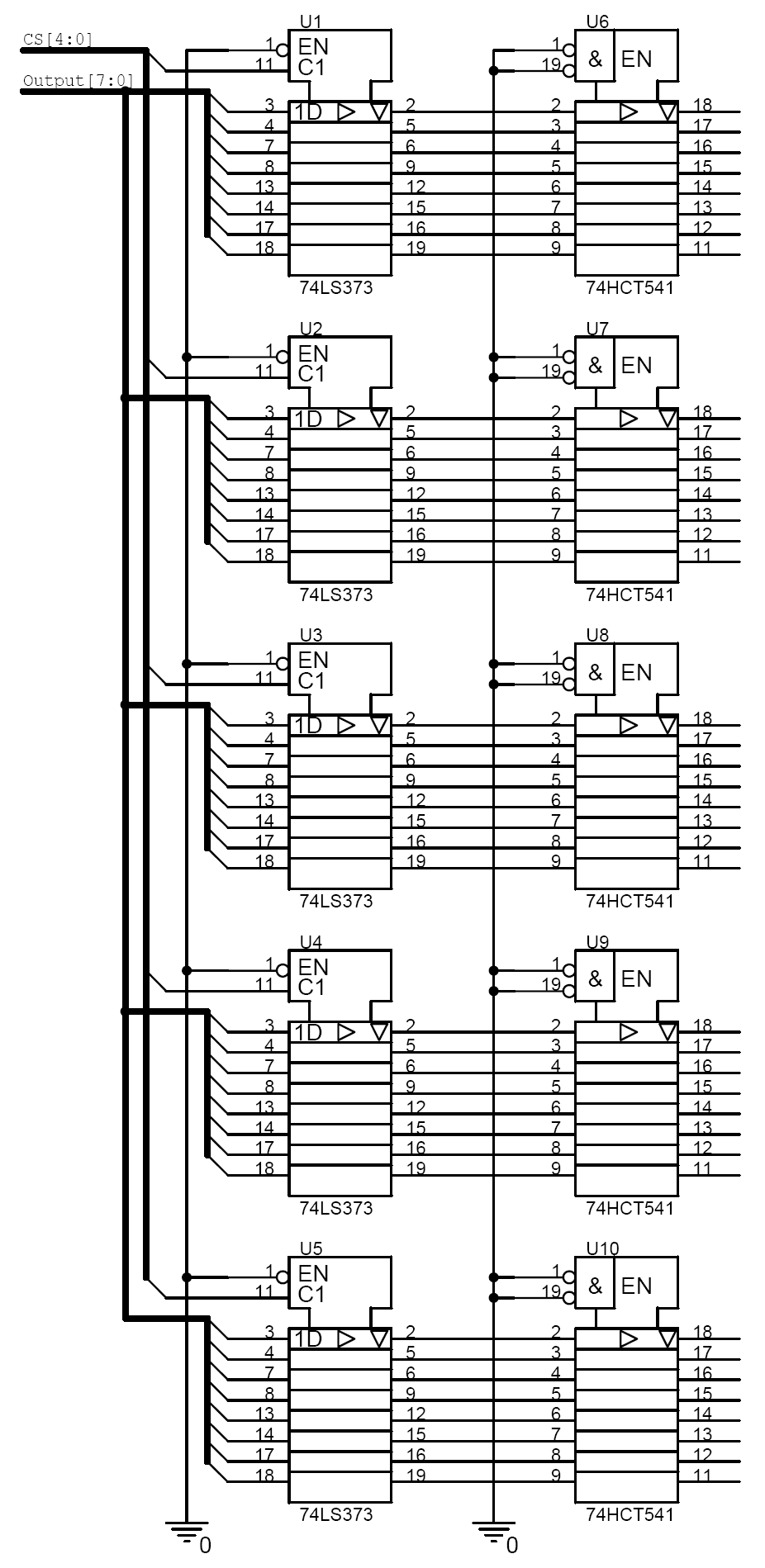
Click on image for higher resolution schematic
In the following timing diagram example, we wanted to set the vertical offset voltage to 0xC038 (logical Vs=-2.51V, physical Vso=3.75V), trigger voltage to 0x0601 and amplification to 0x00 (1X).
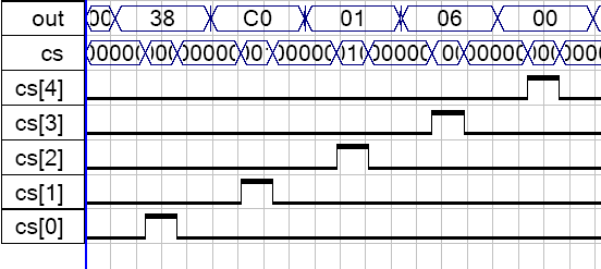
Timing diagram for the output of OutputManager that drove the external circuit (1 cycle)
TriggerManager
This module provides triggering capabilities to the oscilloscope. Without a trigger mechanism, the signal moves very quickly across the screen and is hard or impossible to tell what is going on. The trigger mechanism makes sure that every time the trace is drawn, it is drawn at the same spot, so that the display doesn't flicker randomly.
It was originally decided to incorporate a trigger mechanism with the oscilloscope. The module was written but never incorporated due complications involving memory access and control. Essentially, the trigger mechanism can be programmed to trigger on when the input voltage approached the trigger voltage by a positive edge, negative edge or both.
Integration
All Verilog modules were incorporated into one design which corresponds to the "Controller FPGA" block in the middle of the flow diagram.
The controller clocks the ADC to sample at 8kHz. Details on the ADC0804 can be found on National Semiconductor's website. At this speed, I realised that data can be transmitted real time other the RS232 interface. So why bother with memory management and caching samples in memory you don't need to? So, the controller reads in a value, sends the old value over RS232 while waiting for the current analog to digital conversion to finish.
An additional square wave function generator was placed in the Verilog code to help test the system. The LED indicates communication (on = data sent or received, off = no activity).
Software
As mentioned earlier, the output display for the oscilloscope was done on a computer. Programming in a Windows GUI enviroment is a non trivial task. There's so many things about creating handles, releasing handles, data types and so many things that would make one's head spin. And having fast drawing routines just seemed to be too much to ask for.
So, thinking along the lines of portability and speed, OpenGL naturally comes into mind. With the GLUT (GL utility toolkit), the whole deal with creating windows and event handling becomes portable as well. The software program was divided into 3 sections:
All source code should be viewed with 4 space hard tabs.
- Viewer - Creates windows, handles events, draws traces
- Download Viewer.cpp and Viewer.h
- There are many comments documenting the parameters to OpenGL functions for you to play around with
- Oscilloscope - A class with wrapper functions to access low level functions
- Download Oscilloscope.cpp and Oscilloscope.h
- The argument taken by the constructor (buffer size) doesn't do anything yet
- Pluto - Low level functions that deal with communication over RS232 interface
- Zip file with all the sources and the compiled executable
- Download ViewerSRC.zip
- Compiled for Win32 i386
Keys for using the oscilloscope viewer:
- A - change probe attenuation settings
- L - toggle line drawing
- P - pause
- Alt + Left/Right arrow - zoom in and out horizontally
- Alt + Up/Down arrow - zoom in and out vertically
- Shift + Up/Down arrow - move trace up or down quickly
- Up/Down arrow - move trace up or down slowly
Construction
So finally, details about the construction. The bill of materials is as follows:
| Item | Quantity | Unit Cost |
|---|---|---|
| 7808 | 1 | 0.70 |
| 7805 | 1 | 0.70 |
| 7809 | 1 | 0.80 |
| 50Ω trimpot | 3 | 0.25 |
| 22μF 20V capacitor | 3 | 0.25 |
| 510Ω 1/4W resistor 5% | 2 | 0.01 |
| 300Ω 1/4W resistor 5% | 1 | 0.01 |
| Item | Quantity | Unit Cost |
|---|---|---|
| LF347 | 2 | 1.40 |
| 4067 | 1 | 1.20 |
| ADC0804 | 1 | 4.80 |
| R (1.5kΩ) 1/4W resistor 1% | 30 | 0.05 |
| 2R (3kΩ) 1/4W resistor 1% | 34 | 0.05 |
| 10kΩ 1/4W resistor 1% | 6 | 0.05 |
| 20kΩ 1/4W resistor 1% | 8 | 0.05 |
| 50kΩ 1/4W resistor 1% | 1 | 0.05 |
| 100kΩ 1/4W resistor 1% | 1 | 0.05 |
| 200kΩ 1/4W resistor 1% | 1 | 0.05 |
| 500kΩ 1/4W resistor 1% | 1 | 0.05 |
| 1MΩ 1/4W resistor 1% | 1 | 0.05 |
| Item | Quantity | Unit Cost |
|---|---|---|
| FPGA board (recommended: Pluto) | 1 | 70.00 |
| 74LS373 or any 8 bit latch or flip flop | 5 | 1.20 |
| 74HCT541 or any 8 bit CMOS buffer | 5 | 1.20 |
| 220Ω 1/4W resistor 5% | 5 | 0.01 |
| Item | Quantity | Unit Cost |
|---|---|---|
| Wire | A lot | 0.05 per foot |
| Decoupling capacitors | Some | 0.10 to 0.35 |
| Dual rail power supply | 1 | 20 to 500 |
| Headers (optional) | Some | 0.30 for a row of 30 pins |
| Breadboard (optional) | Some | 10 |
The total comes to about $40CAD after taxes (living in Ontario) without the FPGA board but with 40ft of wire and 20 decoupling capacitors. If you include the FPGA board, the headers, a computer power supply and 5 breadboards (what I used), the total comes to about $120CAD (including taxes and S/H).
The specific values for decoupling capacitors were not mentioned because they vary by application. Try ones in the range of 2nF to 2μF. You would want a bigger one to ripple filter the power supply of a logic device but a smaller one to filter out high frequency noise from the input lines.
All the modules were constructed seperately and merged. Here are a few pictures:
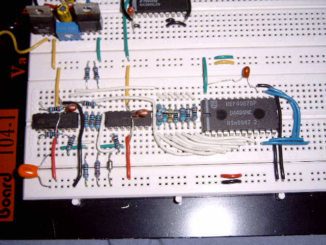
Vertical shift and variable gain amplifier
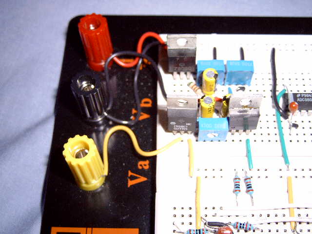
Higher precision power supply
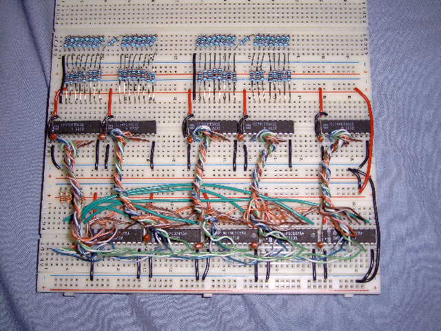
External logic to the OutputManager module
As you can probably tell from the pictures, I put decoupling capacitors everywhere. Many sections may be running at high frequencies, especially the +5V source due to the high speed digital circuits. No prefabricated jumper wire kit was used as I firmly believe that makes one uncool. All wires and leads were cut to length when fitted to the breadboard. For the 8 bit parallel buses, I used RJ45 wire, which conveniently comes in 8 strands and is semi braided.
There's a lot of talk about how opamp circuits are supceptable to noise and how all components should be placed as close to the opamp as possible. So I did that, but seeing how this was built on a breadboard, I somewhat doubt its effectiveness.
Being paranoid, I put in a 5.1V zener diode between the output voltage Vadc and ground. This should prevent me from frying my ADC although the ADC0804 already have built in zener protection.
Analysis
At 1X amplification and 0 vertical offset, a frequency response test was done on the analog circuit. A 10Vp-p sine wave was applied and the output (Vadc) was measured. The results are summarized in the following table:
| Frequency (Hz) |
Vadc (Vp-p) |
Phase shift (degrees) |
|---|---|---|
| 100 | 5.00 | 0 |
| 1k | 5.00 | 0 |
| 10k | 5.00 | 0 |
| 100k | 5.07 | 30.2 |
| 1M | 3.25 | 11.5 |
I guess it full filled my requirement specs. Although the phase shift at 100k is quite noticeable, its not detectable at 10k which is way faster then the nyquist frequency.
At higher amplifications, it was noticed that the signal was not amplified as expected. Infact, it fell significantly short. A thorough test revealed that the resistance across the variable resistor Rf was significantly lower then expected (1MΩ registered as 220kΩ on multimeter). This was due to non-ideal behaviour of the 4067 multiplexer IC. Future versions of the oscilloscope should solve the variable gain amplifier using another method.
Due to a near by power rail driving a high frequency digital circuit, the input to the ADC was very noisy. By putting in a small decoupling capacitor, this problem was fixed. Theoretically this would filter out high frequency signals as well, but we're going at 4kHz, so we're not missing much.
The +8.5V and -8.5V power supply appears to function fine. It was calibrated once and the output voltage did not drift detectably over 1 hour of operation. However, the +5V power supply has a significant load measured to be 0.4A which translates to 2.8W. Thermal stress was noticeable to but did not cause damage to the regulator or its surroundings. The difference between the power supply output with no load, loaded and loaded at high frequency was very significant. Hence, the +5V power supply was calibrated to about +5.1V with a nominal load to insure proper operation when loaded.
Here are a few pictures of the oscilloscope running:
10Hz square waves off the onboard function generator
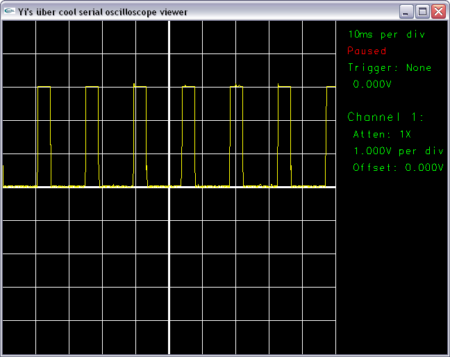
100Hz square waves off the onboard function generator
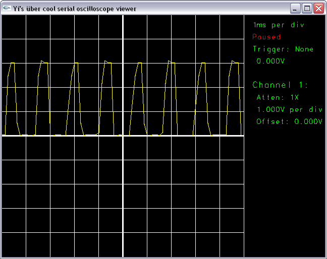
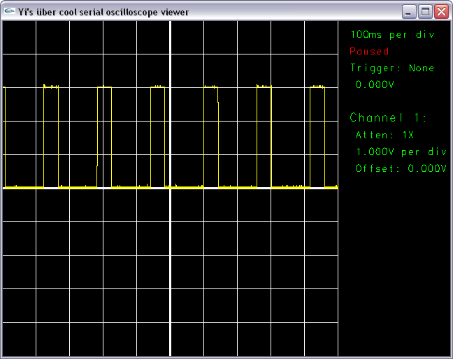
1kHz square waves off the onboard function generator (notice the deterioration of the trace due to sampling rate)
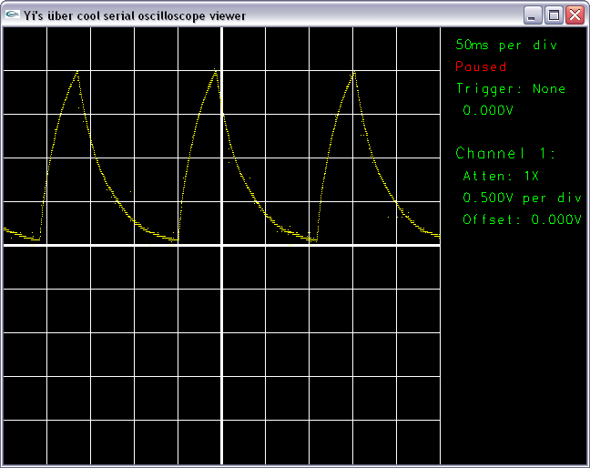
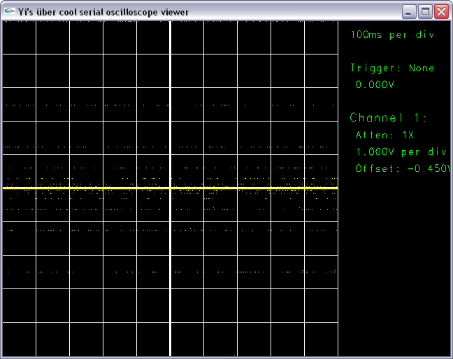
Capacitor charging and discharging (2.2μF and 10kΩ)
The word "testing" spoken into a condensor microphone
The word "testing" spoken into a condensor microphone without connecting lines
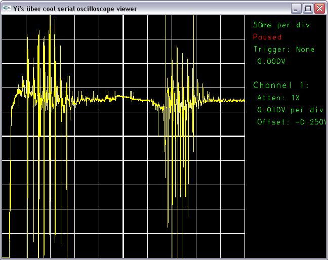
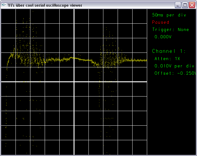
Data captured seemed to be fine if the signal voltage is far from 0V. When the signal is close to 0V (ie with in 1/5 of a div from the zero), I get very funny noise. I still don't know the cause of this noise. Any insight to this problem would be nice. Please contact me me if you have an idea.
Example of funny noise when trace is centred around 0
Files
Here are the files you may want to download:
- Verilog code and RBF for all modules and integration
- Source code and executable for OpenGL interface
- Download source and runtime for GLUT here.
Future Plans
As with all designs, this oscilloscope can be greatly improved. I suggest the following:
- Integrate trigger mechanism
- It really sucks having to pause the screen to see a steady trace
- Implement horizontal shift feature in program
- It sucks even more to have to pause the capture at the right moment to see the trace you want
- Put this on a PCB
- Bread boards are notorious for noise, unwanted inductance, capacitance and contact resistance
- Faster sampling rate
- Maxim sent me some really fast 100Msps ADC's which would be suitable
- Have more reliable variable gain circuit
- Add math functions to the program
- Add, subtract, FFT, integrate, differentiate, peak, period, frequency, etc.
- Use an external LCD display
- I got a few surplus LCD blackout displays and PDA displays and it would be nice to put them to good use
- Add logic analyzer feature
- Port the source to Linux and PalmOS
- I want to walk around with an oscilloscope in my pocket
- Add FPS feature in the program
- Know exactly how accrate the data is and if any data was truncated on transmission
- Implement the second channel with electrical isolation
- And the XY plot mode as well
Please contact me if you have other cool ideas.
This page was last revised on an unknown date.
![]()
